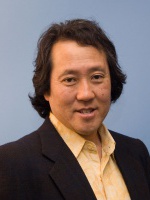
 Nobuhiko Kobayashi
Department of Electrical Engineering
UC Santa Cruz
1156 High St
Santa Cruz, CA, 95064
831-459-3571
You can e-mail Nobuhiko Kobayashi directly through this web site.
Areas of Interest in Materials: Experimental studies on vapor phase growth of semiconductor materials, Structural, optical and electrical characterization of semiconductor materials, Design and fabrication of electronic, optoelectronic, and photonic devices
Material growth capability:
1. MOCVD for group III-As and III-P and related alloys (ASL),
III-Sb and related alloys (Delaware), metal oxides (Delaware)
3. ALD for metal oxides (ASL, Delaware)
Vapor transport deposition system for metal oxide (ASL)
Material characterization capability:
- Scanning electron microscope/EDS (ASL/MACS)
- X-ray photoemission spectroscope/EDS/EELS (ASL/MACS)
- Transmission electron microscope (ASL/MACS)
- Atomic force microscope (ASL/MACS)
- Solar simulator (ASL/MACS)
- Spectroscopic photoconduction measurement system (ASL/MACS)
- Micro FTIR (HPL)
- UV-VIS-NIR spectrometer (HPL)
- Contact angle /surface energy measurement system (HPL)
- x-ray diffraction system (HPL)
Device fabrication capabilities (photolithography, nanoimprinting lithography, sputtering (various metals), thermal evaporator (various metals), e-beam evaporator (various metals), plasma enhanced chemical vapor deposition (SiOx, SiNz, amorphous Si), atomic layer deposition system for metal oxides, all in clean room (HPL)
- Spectroscopic Ellipsometer (HPL)
- Hall measurement system (HPL)
- Probe station/semiconductor parameter analyzer (ASL)
Present topics of study: growth and characterization of group III-V compound semiconductor nanowires for solar cells and thermoelectric devices, deposition and characterization of transition metal oxides for bistable switching devices, deposition and characterization of metal oxides (e.g., CuO) for sensors and metal interconnects.